Affichage des articles dont le libellé est Graphène. Afficher tous les articles

lundi 16 septembre 2013

Graphene could yield cheaper optical chips

In a new graphene-on-silicon photodetector, electrodes (gold) are deposited, slightly asymmetrically, on either side of a silicon waveguide (purple). The asymmetry causes electrons kicked free by incoming light to escape the layer of graphene (hexagons) as an electrical current. Credit: RESEARCHERS


Graphene—which consists of atom-thick sheets of carbon atoms arranged hexagonally—is the new wonder material: Flexible, lightweight and incredibly conductive electrically, it's also the strongest material known to man.

In the latest issue of Nature Photonics, researchers at MIT, Columbia University and IBM's T. J. Watson Research Center describe a promising new application of graphene, in the photodetectors that would convert optical signals to electrical signals in integrated optoelectronic computer chips. Using light rather than electricity to move data both within and between computer chips could drastically reduce their power consumption and heat production, problems that loom ever larger as chips' computational capacity increases.

Optoelectronic devices built from graphene could be much simpler in design than those made from other materials. If a method for efficiently depositing layers of graphene—a major area of research in materials science—can be found, it could ultimately lead to optoelectronic chips that are simpler and cheaper to manufacture.

"Another advantage, besides the possibility of making device fabrication simpler, is that the high mobility and ultrahigh carrier-saturation velocity of electrons in graphene makes for very fast detectors and modulators," says Dirk Englund, the Jamieson Career Development Assistant Professor of Electrical Engineering and Computer Science at MIT, who led the new research.

Graphene is also responsive to a wider range of light frequencies than the materials typically used in photodetectors, so graphene-based optoelectronic chips could conceivably use a broader-band optical signal, enabling them to move data more efficiently. "A two-micron photon just flies straight through a germanium photodetector," Englund says, "but it is absorbed and leads to measurable current—as we actually show in the paper—in graphene."

Unbiased account

As Englund explains, the problem with graphene as a photodetector has traditionally been its low responsivity: A sheet of graphene will convert only about 2 percent of the light passing through it into an electrical current. That's actually quite high for a material only an atom thick, but it's still too low to be useful.

When light strikes a photoelectric material like germanium or graphene, it kicks electrons orbiting atoms of the material into a higher energy state, where they're free to flow in an electrical current. If they don't immediately begin to move, however, they'll usually drop back down into the lower energy state. So one standard trick for increasing a photodetector's responsivity is to "bias" it—to apply a voltage across it that causes the electrons to flow before they lose energy.

The problem is that the voltage will inevitably induce a slight background current that adds "noise" to the detector's readings, making them less reliable. So Englund, his student Ren-Jye Shiue, Columbia's Xuetao Gan—who, together with Shiue, is lead author on the paper—and their collaborators instead used a photodetector design developed by Fengnian Xia and his colleagues at IBM, which produces a slight bias without the application of a voltage.

In the new design, light enters the detector through a silicon channel—a "waveguide"—etched into the surface of a chip. The layer of graphene is deposited on top of and perpendicular to the waveguide. On either side of the graphene layer is a gold electrode. But the electrodes' placement is asymmetrical: One of them is closer to the waveguide than the other.

"There's a mismatch between the energy of electrons in the metal contact and in graphene," Englund says, "and this creates an electric field near the electrode." When electrons are kicked up by photons in the waveguide, the electric field pulls them to the electrode, creating a current.

Hot topic

In experiments, the researchers found that, unbiased, their detector would generate 16 milliamps of current for each watt of incoming light. Its detection frequency was 20 gigahertz—already competitive with germanium. (Some experimental germanium photodetectors have achieved higher speeds, but only when biased.) With the application of a slight bias, the detector could get up to 100 milliamps per watt, a responsivity commensurate with that of germanium.

Englund is confident that better engineering—thinner electrodes, or a narrower waveguide—could yield a photodetector whose responsivity is even higher. "It's a matter of engineering," he says. "We are already testing some new tricks to get another factor of two or four."

"I think it's great work," says Thomas Mueller, an assistant professor at the Vienna University of Technology's Photonics Institute. "The main drawback of graphene photodetectors was always their low responsivity. Now they have two orders of magnitude higher responsivity, which is really great."

"The other thing that I like very much is the integration with a silicon chip," Mueller adds, "which really shows that, in the end, you'll be able to integrate graphene into computer chips to realize optical links and things like that."

In fact, the same issue of Nature Photonics also features a paper by Mueller and colleagues, reporting work very similar to that conducted by Englund and his team. "We did not know that we were doing the same thing," Mueller says. "But I'm very happy that two papers are coming out in the same journal on the same topic, which shows that it's an important thing, I think."

The chief difference between the two groups' work, Mueller says, is that "we used slightly different geometry." But, he adds, "Honestly, I think that Dirk's geometry is more practical. We were also thinking about the same thing, but we didn't have the technical capabilities to do this. There's one process that they do that we were not able to do."

Journal reference: Nature Photonics

Provided by Massachusetts Institute of Technology

September 16, 2013

24 minutes ago by Larry Hardesty

Read more at: http://phys.org/news/2013-09-graphene-yield-cheaper-optical-chips.html#jCp

mardi 27 août 2013

KAIST Develops a Metal-Graphene Composite Material Hundreds of Times Stronger Than Pure Metals


Graphene © AlexanderAlUS/CORE Materials

Researchers from the Korea Advanced Institute of Science and Technology (KAIST) have developed a new metamaterial that is proven to be hundreds of times stronger than pure metals. To maximize the potential increase in strength provided by the use of graphene, the KAIST team created a multi-layered structure, alternating layers of graphene and metal—this composite nanomaterial consists of graphene inserted into copper and nickel. The resulting metal-graphene multilayer composite material is the first of its kind, and the team’s research was published in the science journal, Nature Communications in July of 2013.


Nuclear Reactor © Tysh

To build this structure the team utilized a process called Chemical Vapor Deposition (CVD) allowing them to grow a single layer of graphene on a metal deposited substrate. The team then deposited another layer of metal on top of the graphene, and the two step process was repeated to add additional layers to create the new composite.

To measure the strength of the new material, the team conducted a series of micro-compression tests administered through a Transmission Electronic Microscope and Molecular Dynamics Simulation. The results showed the composite material’s ability to block dislocations and cracks caused by external damage traveling inwards to be much greater than that of conventional metal-metal multilayered materials. The increase in strength varied depending on the interlunar distance, with 70nm exhibiting 500 times more strength than pure copper, and 100nm measuring to be 180 times stronger than pure nickel. A clear relationship between the interplanar distance and the strength of the material was identified. It was also concluded that the smaller interplanar distance made dislocation more difficult, thus resulting in a stronger material.

Seung Min Han, the KAIST professor who led the research team to success commented “the result is astounding as 0.00004% in weight of graphene increased the strength of the materials by hundreds of times” and that “improvements based on this success, especially enabling mass production with roll-to-roll process or metal sintering process, in the production of automobile and spacecraft lightweight, ultra-high strength parts may become possible.” He went on to explain how the new material could also be applied to coating material for the construction of nuclear reactors and products that require a high level of reliability.

+ KAIST

mercredi 21 août 2013

3-D Graphene — The Future Of Solar Cells?

3-D graphene can function as an effective — and very economical — substitute for the platinum that is commonly used in dye-sensitized solar cells, according to new research from Michigan Technological University. By substituting the newly created and relatively cheap material known as three-dimensional graphene for the very expensive and rare element of platinum the researchers think that the cost of dye-sensitized solar cells can be cut significantly.

Dye-sensitized solar cells (DSSCs) are a very promising type of solar cell that are easy to produce, flexible, and relatively efficient at converting solar energy into electricity. As they are currently produced, though, they rely on a number of relatively expensive materials, such as platinum — platinum currently sells for somewhere around $1500 an ounce, so if a cheaper material could be found to replace platinum then the total cost of producing DSSCs could no doubt be reduced significantly. That’s where 3-D graphene comes in. The newly created material can effectively replace platinum in DSSCs without diminishing their efficiency.

“A field emission scanning electron microscopy (FESEM) image of 3D honeycomb-structured graphene. The novel material can replace platinum in dye-sensitized solar cells with virtually no loss of generating capacity.” Image Credit: Hui Wang

The press release from Michigan Technological University provides details on the new material:

Regular graphene is a famously two-dimensional form of carbon just a molecule or so thick. Yun Hang Hu, the Charles and Caroll McArthur Professor of Materials Science and Engineering, and his team invented a novel approach to synthesize a unique 3D version with a honeycomb-like structure. To do so, they combined lithium oxide with carbon monoxide in a chemical reaction that forms lithium carbonate (Li2CO3) and the honeycomb graphene. The Li2CO3 helps shape the graphene sheets and isolates them from each other, preventing the formation of garden-variety graphite. Furthermore, the Li2CO3 particles can be easily removed from 3D honeycomb-structured graphene by an acid.

The researchers determined that the 3D honeycomb graphene had excellent conductivity and high catalytic activity, raising the possibility that it could be used for energy storage and conversion. So they replaced the platinum counter electrode in a dye-sensitized solar cell with one made of the 3D honeycomb graphene. Then they put the solar cell in the sunshine and measured its output. The cell with the 3D graphene counter electrode converted 7.8% of the sun’s energy into electricity, nearly as much as the conventional solar cell using costly platinum (8%).

The researchers note that the process of synthesizing the 3-D honeycomb graphene is relatively cheap and easy — there are no significant barriers to its wider adoption. As they put it: “Making it into a counter electrode posed no special challenges.”

The research has been funded by both the American Chemical Society Petroleum Research Fund and the National Science Foundation.

Published on August 21st, 2013 | by Nathan

Scientists Take Graphene to the Next Level

Photograph by Wei Long/EPA

Graphene—the thinnest, toughest material ever produced—conducts electricity 30 times faster than silicon

Graphene! Graphene! Miracle of miracles! Savior of technology!

At least, that’s been the chatter for the last nine or so years, ever since scientists isolated the single-atom-thick carbon derivative. Graphene is so light, you see—so strong, you understand—that it will bring us the Space Age we were always promised. It will also apparently cure cancer, solve the Palestinian-Israeli conflict, and settle the CBS (CBS)-Time Warner Cable(TWC)throwdown.

And that’s great. But all this is in theory. Show me something real, scientists. I mean, I also was down with cold fusion, Betamax, and Duke Nukem Forever, so I know from disappointment.

Thing is, those scientists seem to have actually reached an important breakthrough with graphene. According to a post today in MIT Technology Review, a group of really smart people appear to have solved a major problem with using graphene in transistors by making it act like a switch. That’s something critical to information processing—and so far, something graphene was not able to do.

Graphene is wickedly conductive, which is important. A graphene transistor was clocked at 427 GHz. Not to get all Doc Brown on it—427 GHZ!—but that’s insane in the membrane (i.e., insane in the brain). An 11-inch MacBook comes with a stock processor running at 1.3 GHz. So a graphene-based processor, in theory, could run 300 times that. Zoom-zoom, know what I’m sayin’?

Until now, graphene had this … issue. You couldn’t turn it off. And if you know anything about transistors, you know that turning on and off is sort of a transistor’s raison goddamn d’etre. So while graphene is super-fresh and all that, if it can’t turn on and off, the question of its efficacyis moot. But aforementioned scientists have been able to come up with an entirely different way of getting graphene to work in a transistor. The result is “a system that dramatically outperforms silicon,” says the article. “[The researchers] say the performance is ‘several orders of magnitude higher than for any reported or even projected scaled circuits.’”

There used to be a lot of hand-wringing that we were running up against the upper limits of Moore’s Law when it came to processing power. If we’re talking about silicon, that may be true. But if this graphene stuff is legit, tomorrow’s processors will make today’s look as they were made by Fisher-Price (MAT).
Grobart is a senior writer for Bloomberg Businessweek. Follow him on Twitter @samgrobart.

By Sam Grobart

August 20, 2013

mardi 13 août 2013

Secret Of Graphene Revealed: It’s A Total Diva


A team at Lawrence Berkeley National Laboratory has just announced a new breakthrough in the field of graphene research, leading to the next generation of high-efficiency solar cells, computers and other advanced technologies. Graphene, a new material that was discovered less than 10 years ago, is an ultra-thin, superstrong, superflexible electron conductor. As for how to explain the Berkeley Lab research in lay terms, let’s just say that if graphene had a personality it would have its own reality show, and it would give Total Divasa run for the money.

No, seriously. Researchers have already demonstrated that graphene possesses an outsized talent for showing off its unique properties, which is surely one prerequisite for diva-ness. The other is a highly developed sensitivity to minor irritations, and that is the focus of the new Berkeley Lab research.

A Graphene Mystery

To understand the significance of the Berkeley Lab breakthrough, let’s start at the beginning. Graphene consists of a sheet of carbon only one atom thick, with a distinctive lattice structure similar to chicken wire.


Dirac spectrum in bilayer graphene courtesy of LBL.

On the plus side, graphene is an extremely efficient conductor, far more efficient than silicon. However, this is where graphene’s diva side kicks in. To translate graphene into on/off devices, you need to be able to switch off the conduction, and graphene simply refuses to shut itself down completely.

The basic problem is that a single sheet of graphene has no range of energy that prohibits electrons from existing. Called a bandgap, this range is essential for controlling the electron current.

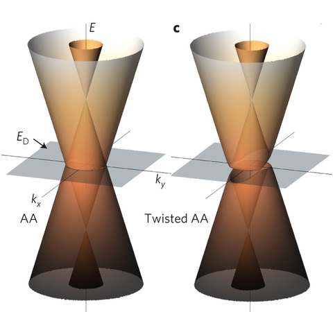
Berkeley Lab researchers previously attempted to work around the problem by using two layers of graphene to create a bandgap. However, when the bilayer graphene was incorporated into devices it flopped. The devices acted as if the graphene was a single layer, with no bandgap.

Mystery, Solved!

Picking apart that phenomenon is the next critical phase in the research, and that is where the new Berkeley Lab research project comes in.

Using the Lab’s Advanced Light Source, they subjected the bilevel graphene to a beam of X-ray photons. That analytic tool produces a snapshot of the material’s electronic spectrum.

The results were surprising. In contrast to what the team had assumed, the spectrum contained extra branches. These consisted of massless Dirac fermions, which are electrons that behave like photons (named after U.K. physicist Paul Dirac). Since Dirac fermions do not follow the same bandgap rules as normal electrons, that explains why the bilayer graphene had no “on-off” switch.

The team traced the creation of massless Dirac fermions to atomic-level misalignments between the two layers of graphene. While almost imperceptible, the misalignment creates a “twist” in the material that generates the massless Dirac fermions.

The bad news is, the problem is not easily resolved. The team estimates that just ten atomic “misfits” per square micron are enough to throw the whole thing off.

However, the team anticipates that the results will guide it to the next step in the research. Lead author of the study Keun Su Kim explains:

Now that we understand the problem, we can search for solutions. For example, we can try to develop fabrication techniques that minimize the twist effects, or reduce the size of the bilayer graphene we make so that we have a better chance of producing locally pure material…

Kim also sees the study applying across the field of graphene research:

A lesson learned here is that even such a tiny structural distortion of atomic-scale materials should not be dismissed in describing the electronic properties of these materials fully and accurately.

More Exciting News About Graphene

As mentioned above, graphene has only been around since 2004, when a U.K. research team literally lifted a layer of atoms from the surface of a chunk of graphite with sticky tape, but the topic has already generated thousands of research papers as scientists race to unlock the mysteries of its unique properties.

Among the many recent developments, researchers are beginning to identify materials that mimic graphene’s more desirable properties, while being more capable of taking direction and put up with minor irregularities. A team at Columbia University, for example, used boron nitride (aka “white graphene”) to create the rare “Hofstadter butterfly” fractal pattern (a fractal pattern repeats itself in smaller and smaller shapes).

A research team in Spain went even farther afield, finding that they could develop an acoustic analog for graphene simply by drilling holes in a sheet of plastic.

As for why CleanTechnica is so interested in graphene (see our numerous posts on the topic), photovoltaic cells are among the many devices that could be looking at an ultra-efficient graphene future.

Published on August 13th, 2013 | by Tina Casey

vendredi 9 août 2013

Un capteur photo en graphène

Nanyang Technological University (NTU), à Singapour, vient d'inventer un nouveau type de capteur qui permettra de prendre des photos nettes et claires même avec une faible luminosité. Ce nouveau capteur, constitué de graphène, est considéré comme le premier capable de détecter un large spectre de lumière, depuis le visible jusqu'à l'infrarouge moyen, et cela avec une haute sensibilité. Cela rend les applications très nombreuses, notamment àtout type d'appareil photo, y compris les appareils infrarouges, les satellites et bien d'autres.

Représentation du graphène
Le capteur en graphène a l'avantage d'être 1000 fois plus sensible à la lumière que les capteurs classiques, mais il utilise également 10 fois moins d'énergie car il fonctionne à un plus bas voltage. Produit en grande quantité, ce capteur pourrait coûter au moins cinq fois moins cher que les capteurs d'aujourd'hui. Le graphène est un million de fois plus fin qu'un cheveu humain, il ne fait en réalité qu'un atome d'épaisseur et est un assemblage d'atomes de carbone selon un schéma hexagonal. Mais le graphène est également connu pour d'autres propriétés comme sa grande conductivité électrique, sa flexibilité et sa durabilité.

L'Assistant Professor Wang Qijie de NTU School of Electrical & Electronic Engineering, est l'inventeur de ce capteur, et a déclaré penser être le premier à développer un capteur à large spectre et haute sensibilité en utilisant du graphène pur. Ce capteur a également été développé tout en gardant à l'esprit les techniques actuelles de fabrication, ce qui devrait permettre aux industriels de continuer à utiliser les procédés des capteurs CMOS (Complementary Metal-Oxyde-Semiconductor) qui dominent aujourd'hui ce marché. Il suffira simplement de remplacer le matériau de base du capteur photo par les nouvelles nanostructures de graphène.

Si cette innovation est adoptée par l'industrie, cela pourrait mener à la baisse des prix des appareils photo et à l'augmentation de la durée de vie de leurs batteries.


Source: BE Singapour numéro 85 (31/07/2013) - Ambassade de France à Singapour / ADIT - http://www.bulletins-electroniques.com/ ... /73652.htm
Illustration: Carbophiliac

Posté par Adrien le Vendredi 09/08/2013 à 00:00

mercredi 31 août 2011

Découvertes sur les propriétés de liaison entre le graphène et l'iridium

Le graphène est un cristal bidimensionnel (monoplan) constitué d'une unique couche d'atomes de carbone ordonnés selon une structure hexagonale plane. Il a été isolé pour la première fois en 2004 par le néerlandais Andre Geim, du département de physique de l'université de Manchester. Cette découverte a été récompensée en 2010 par le prix Nobel de physique. Par rapport à l'acier, une feuille de graphène est six fois moins dense, deux fois plus dure, et 13 fois plus rigide au pliage. Sur sa surface, les électrons se déplacent à une vitesse plus rapide que dans n'importe quel autre matériau.

Une méthode très répandue consiste à produire le graphène directement sur des surfaces métalliques. Comme le graphène possède des liaisons chimiques fortes avec de nombreux métaux, l'étape consistant à le détacher de ces derniers afin de l'isoler peut conduire à sa destruction. Une équipe de l'Université de Cologne, en coopération avec des chercheurs de Jülich (Rhénanie-du-Nord-Westphalie), Zagreb et Grenoble, a alors découvert que cet effet ne se produit pas lorsque le métal utilisé est l'iridium [1].

En effet, les chercheurs sont parvenus à mesurer la distance de liaison entre le graphène et l'iridium avec une précision représentant un centième du diamètre d'un atome. Ils ont pu constater que cette distance est bien plus élevée que pour d'autres métaux, d'où une plus faible liaison chimique entre les deux éléments. Ces mesures ont été menées en grande partie à l'Installation Européenne de Rayonnement Synchrotron (ESRF) de Grenoble.

Les résultats expérimentaux ont été confirmés par des calculs théoriques de l'interaction faible de Van-der-Waals, principale responsable de la liaison entre le graphène et l'iridium. Ces calculs ont été menés sur le supercalculateur JUGENE du Centre de recherche de Jülich, et ont permis pour la première fois de décrire correctement la liaison graphène/iridium de manière théorique.

BE Allemagne 536 >> 25/08/2011

http://www.bulletins-electroniques.com/actualites/67487.htm

mardi 23 août 2011

Du graphène et de l'étain pour des batteries plus performantes


Un nouveau matériau composite, constitué de couches de graphène et d'étain, permet d'envisager la mise au point de batteries à très longue durée de vie, et aux performances accrues

Pour certaines industries, la mise au point de batteries rapidement rechargeables et à longue durée de vie est essentielle. Pour répondre à ce besoin, des chercheurs du Laboratoire de l'Université de Berkeley ont mis au point un nouveau composant aux propriétés extrêmement intéressantes. Synthétisé à partir de feuilles de graphène et d'étain, celui-ci pourrait s'intégrer efficacement à des batteries lithium-ion, augmentant leurs capacités ainsi que leur durée de vie.

Un "sandwich" de graphène et d'étain, aux performances notables

Les chercheurs ont superposé alternativement des micro-feuilles de graphène et d'étain, à la manière d'un mille-feuille. Le produit créé est alors chauffé à plus de 300 degrés celsius. Cette opération a pour effet de faire fondre les feuilles d'étain, dont les atomes se condensent sous forme de piliers. Cette concentration augmente logiquement l'épaisseur des couches en question, accroissant par là même l'épaisseur totale du composé. Or, selon les développeurs, ce changement de volume améliore considérablement les performances du matériau lorsqu'il est intégré à l'électrode d'une batterie. Celle-ci devient plus performante, et s'use moins rapidement.

Un pas de plus pour du stockage d'énergie performant

Le matériau est donc idéal pour la mise au point de batteries lithium-ion pouvant être réutilisées à de très nombreuses reprises. Or, certaines industries de pointe (et notamment celle des véhicules électriques) sont dépendantes des avancées du secteur. Ainsi, comme le souligne Yuegang Zhang, membre de l'équipe de recherche, “le développement de véhicules électriques passe par la mise au point de batteries haute-performances, pouvant être rechargées extrêmement rapidement, et dont la durée de vie ne soit pas altérée par les rechargements successifs”. Le chercheur souligne d'ailleurs que "ce "sandwich" de graphène et d'étain est un pas de plus une technologie de stockage d'énergie ultra-performante".

Publié le 23 août 2011  


http://www.atelier.net/articles/graphene-de-letain-batteries-plus-performantes

mardi 16 août 2011

Une matière à deux dimensions décelée dans l’espace ?

Le télescope Spitzer aurait décelé dans deux galaxies proches un matériau que les scientifiques n’ont obtenu que récemment sur Terre : le graphène.


Le télescope spatial Spitzer aurait détecté la signature du graphène dans les Nuages de Magellan, deux petites galaxies situées non loin de notre Voie Lactée, vient d’annoncer la Nasa. Cette matière est très particulière, puisqu’il s’agit de cristaux de carbone bidimensionnels. L’étude a été publiée dans The Astrophysical Journal Letters.

En plus d’être absolument plat, le graphène est ultra résistant et très bon conducteur d’électricité. Il n’a été obtenu en laboratoire qu’en 2004. Ses découvreurs, Andre Geim et Konstantin Novoselov, ont obtenu le prix Nobel de physique 2010. Il pourrait trouver des applications dans la fabrication de matériel informatique, d’écrans ou de panneaux solaires.

La découverte de graphène dans l’espace ne présente pas d’intérêt direct pour l’industrie, souligne la Nasa. Mais mieux comprendre les réactions chimiques incluant du carbone pourrait éclairer la façon dont se sont développées des créatures qui en sont composées. Donc la vie sur la Terre.

Spitzer, qui scrute le ciel dans l’infrarouge, a décelé le graphène dans les matériaux éjectés par des étoiles mourantes. Au passage, le télescope a déniché des traces de carbone C70 – une première en dehors de notre galaxie.

Source : Nasa / National Optical Astronomy News – Illustration : IAC/NASA/NOAO/ESA/STScI/NRAO

16 août 2011 – 16:56

http://www.nationalgeographic.fr/actualite/astronomie-espace-spitzer-graphen/7910073/